
An avalanche photodiode or APDs is a highly sensitive semiconductor. It is a photodiode detector that uses the photoelectric effect to convert light into electricity. This is a similar structure to regular photodiode but operated at much higher reverse biased conditions.
Japanese engineer Jun-ichi Nishizawa in 1952 first invented the avalanche photodiode (APD). However, before its invention, the study of avalanche breakdown, microplasma defects in Silicon and Germanium, and the investigation of optical detection using p-n junctions exist.
In this piece, we will discuss the structure of APDs, their working, the material used, advantages & disadvantages, and their application.
Structure of Avalanche Photodiode
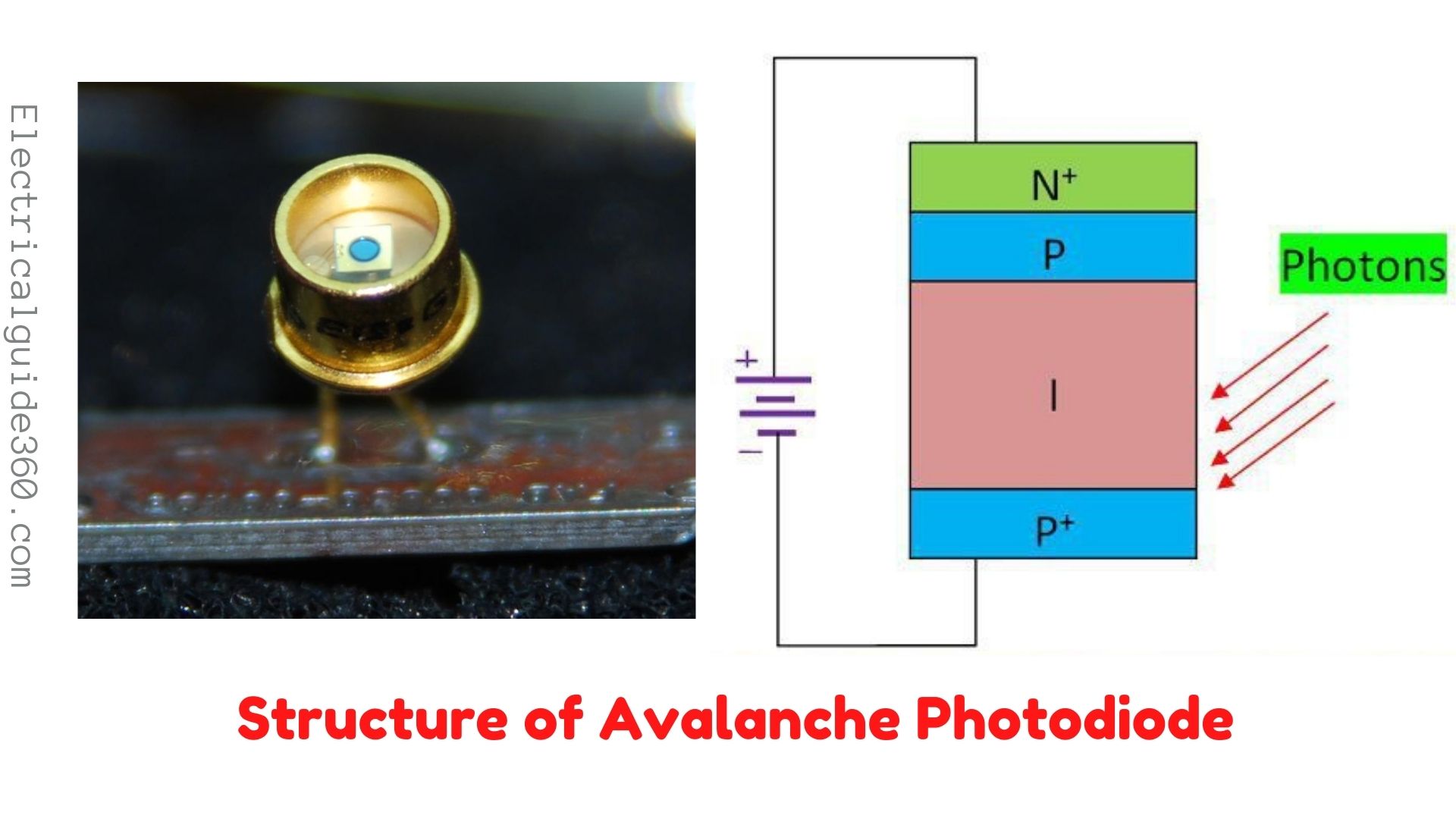 In Avalanche Photodiode, PIN Structure of photodiode is used, where the incident photons generate primary electrons and holes. Avalanche photodiode consists of p+ and n+ region which is heavily doped. Also, there are another two lightly doped regions i.e, intrinsic region (or I) and P region.
So here, the p+ region acts as the anode whereas the n+ region acts as the cathode. Reverse bias is mostly applied across the pn+ region.
Working of Avalanche Photodiode
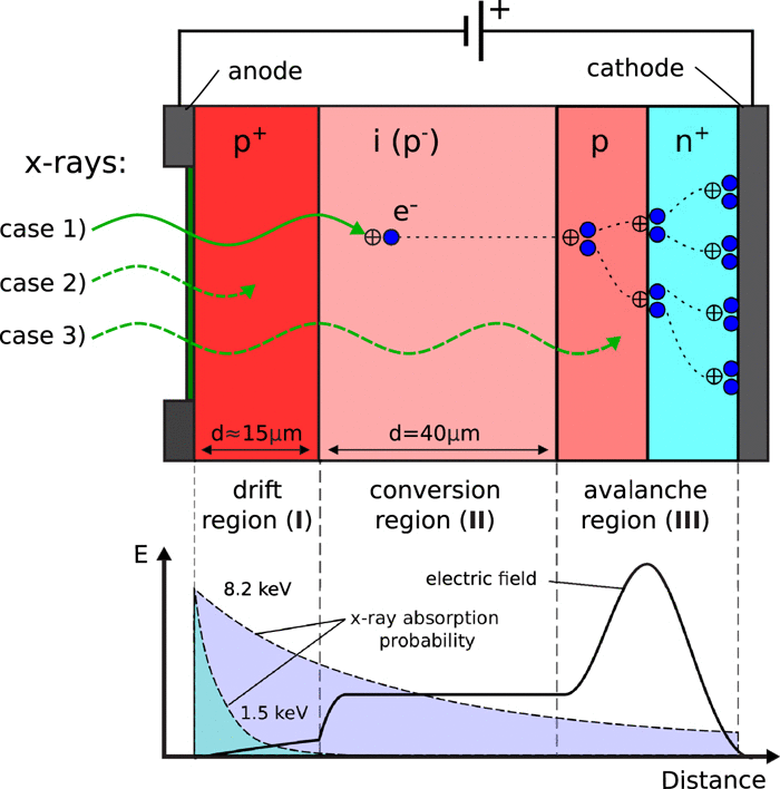
In Avalanche Photodiode, relatively high (around 20v) reversed biased or reversed voltages are applied to the photodiode which accelerates the electrons with high energy. These electrons and holes strike the neutral atoms and separate the other bonded electrons and holes. This is known as a secondary process causing avalanche actions. Thus, one photon eventually generates multiple charge carriers. This means photodiode internally amplifies the photocurrent.
APDs have a quantum efficiency of more than one (10 to 100) which is m times larger than the normal PIN Photodiode where ‘m’ is the multiplication factor or gain factor(10-500).
Performance
The application and performance of APD depend on many parameters. Two of the most important factors are:
- Quantum efficiency:- Which indicates how well incident optical photons are absorbed and then used to generate primary charge carriers;
- The total leakage current:- Which is the sum of the dark current, photocurrent, and noise.
Electronic components with dark noise can be categories into series and parallel noise. The serial noise, which is the effect of the shot noise, is largely proportional to the APD capacitance, while the parallel noise is related to the volumetric APD oscillations and surface dark currents.
Also Learn: What is Homojunction and Heterojunction Semiconductor?
Material Used
The material used for the purpose is Silicon (Si), Germanium (Ge), Indium Gallium Arsenide (InGaAs), Lead sulfide (PbS), Mercury (Hg), Cadmium (Cd), Telluride (Te), Gallium nitride (GaN), mercury cadmium telluride (HgCdTe).
Some of the few purposes of materials used are:
- Silicon (Si) detects in the visible and near-infrared range with little multiplication noise (excessive noise).
- Germany (Ge) will detect infrared radiation up to a wavelength of 1.7 µm, but there is high multiplication noise.
- InGaAs detect up to 1.6 µm in length and have less multiplication noise than Ge.
- Gallium nitride diodes are used to work with ultraviolet light.
- HgCdTe-based diodes work with infrared radiation, typically at wavelengths up to about 14 µm, but require cooling to reduce dark currents. With this material system, very little noise can be achieved.
Advantages
- It is useful in detecting light that has low intensity.
- Sensitivity is high compared to other photodiodes.
- Quick Response.
- One photon eventually generates multiple charge carriers. This means photodiode internally amplifies the photocurrent.
Disadvantages
- Requires High operating voltage.
- During operation, there is an excessive noise that is being produced.
- Output is non-linear.
Applications
Typical applications for APDs are laser rangefinders, long-range fiber-optic telecommunication, and quantum sensing for control algorithms, Antenna Analyzer bridge, LASER scanner, Barcode reader, Speed gun, Laser microscopy, PET scanner.
")


")
 Current Feels Different to a Shock From Direct (DC) Current?")


